
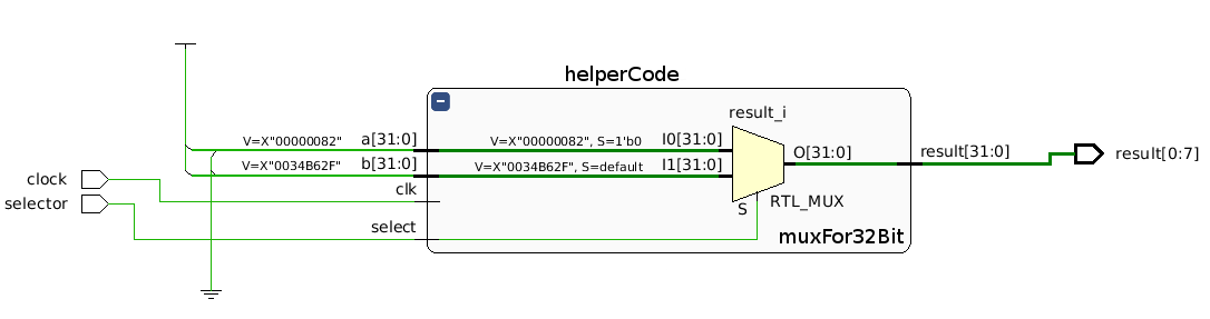
In this week, we designed a 32 bit multiplexer in the lab. You can download the manual for this lab session that sent by our lecturer from this link.
Our purpose is designing a 32 bit multiplexer but our FPGA board has just 8 leds so we could not observe 32 bits. For this problem, we showed just last 8 bits of result via leds on the board. So, we designed a 32 bit multiplexer and another module for get last 8 bits of result from 32 bit multiplexer. Our new module has two inputs (selector, clock) and an output (8 bits of result).
Here are codes:
[code title=”muxFor32Bit.v”]
module multiplexer(
input [31:0] a,
input [31:0] b,
input select,
output [31:0] result,
input clk
);
wire [31:0] a,b;
reg [31:0] result;
always @(a,b,select)
begin
if(select==0)
result=a;
else
result=b;
end
endmodule
[/code]
The code above is a design for 32 bit multiplexer, but we can’t observe 32 bit result on FPGA board because of leds count. We need creating a new module for check the code as I said above. In this module, we must get only last eight bits of the result from multiplexer module and observe value of these leds on the FPGA board.
[code title=”helperCode.v”]
module mainCode(
input selector,
input clock,
output [0:7] result
);
wire [0:31] a,b;
assign a=’d130;
assign b=’d3454511;
wire [0:31] temp;
multiplexer child(a,b,selector,temp,clock);
assign result=8’b11111111 & temp;
endmodule
[/code]
Why we use the clock?
Actually, we don’t need a clock for this design because it is simple. If we have a complex design, we should use a clock for working sync on FPGA board. If we don’t use a clock, some of values from inputs or calculation algorithms may be delayed so the result may be wrong.
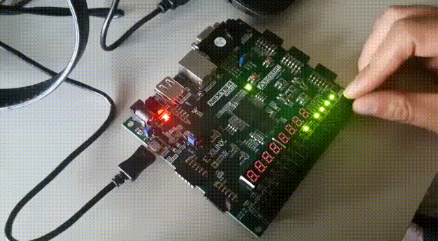
Here is, the design:
Here is, the code is running on the board:
kaimdaim
Hello,
I have resistivity measurement project using 2 DMMs,one for measuring V and the other for I.
Since I prefer to apply dipole-dipole method,I designed a measurement cable connected to 9 probes,in order to stop the measurement at the n6 stage.Thus I read the injected current from the first 2 probes,and I read the potentials from the following probes(C1-C2;P1-P2).Firstly I take the potential readings from P1-P2 as power supply is turned-off.Then I turn on the power supply and I take current readings from C1-C2 and voltage readings from P1-P2.This is repeated for each pairings as told in the figure attached.
|C1|C2||P1|P2|
|1|2| |3|4|
|1|2| |4|5|
|1|2| |5|6|
|1|2| |6|7|
|1|2| |7|8|
|1|2| |8|9|
|2|3| |4|5|
|2|3| |5|6|
|2|3| |6|7|
|2|3| |7|8|
|2|3| |8|9|
|3|4| |5|6|
|3|4| |6|7|
|3|4| |7|8|
|3|4| |8|9|
|4|5| |6|7|
|4|5| |7|8|
|4|5| |8|9|
|5|6| |7|8|
|5|6| |8|9|
|6|7| |8|9|
Finally I have 21 V0,21 V1 and 21 I readings,as a total of 63 readings.
Is it possible to design and apply this switching with esp32 and MUX?And is it possible to record the savings afterall?(The model of DMMs I used is General Tools TS04,which has bluetooth).
unalfaruk
I am sorry, it is too difficult to understand your need and answer your question here.