

This year I’m taking Computer Architecture lesson, in this lesson we learn FPGA so I’m glad because I heard a lot of interesting applications about FPGA, especially about space and aviation. Actually, I still don’t know exactly what is done using FPGA. But I was excited in the lab class because of there is new technology that I can learn 🙂
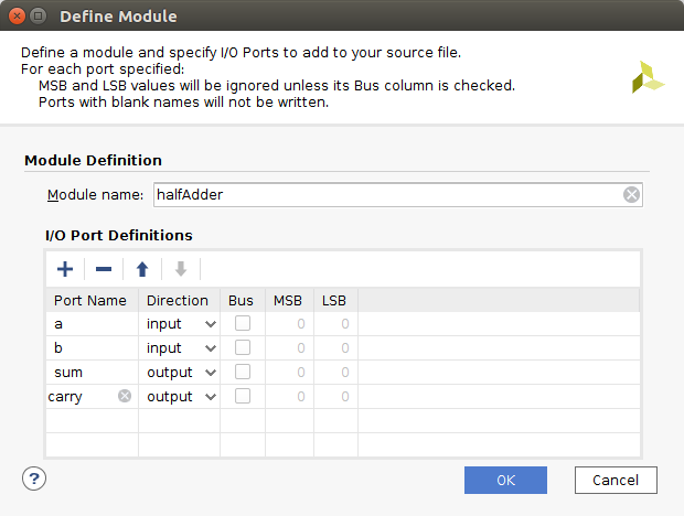
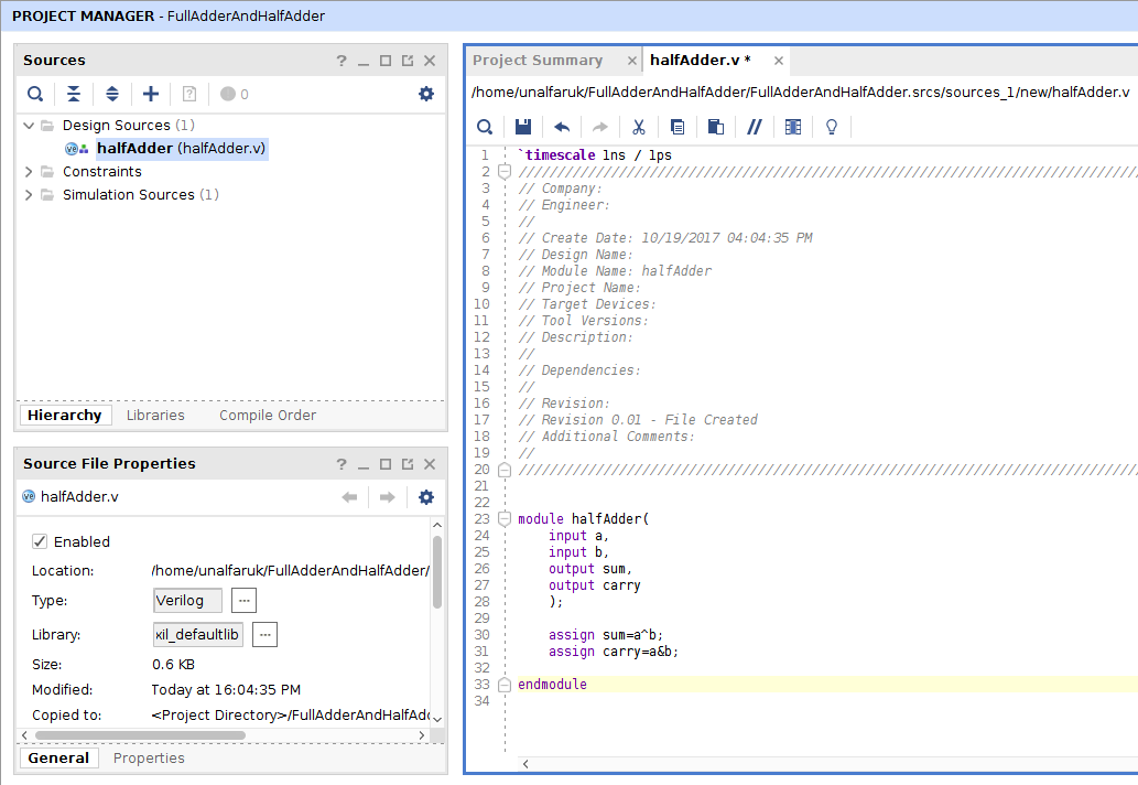
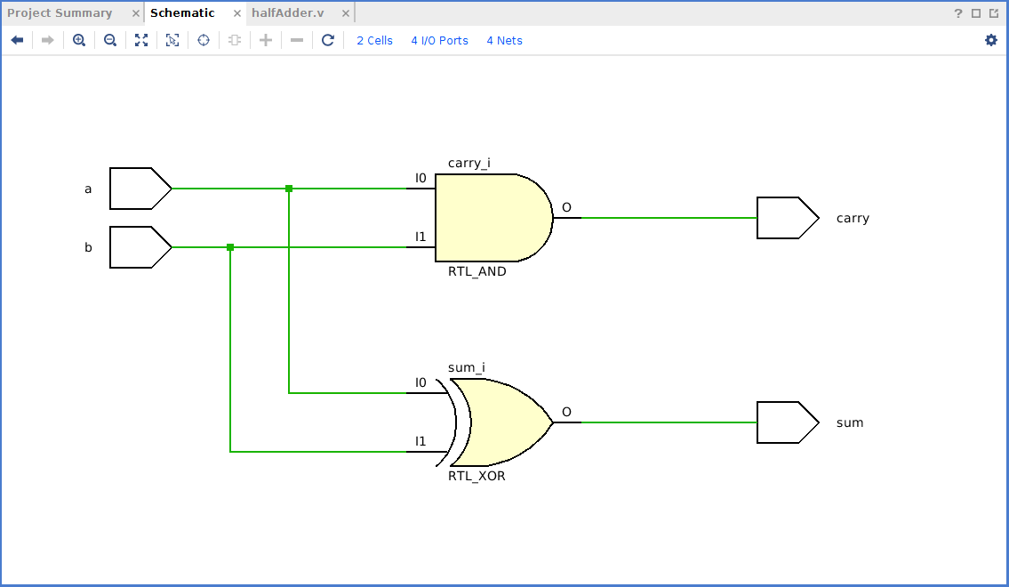
Today, we designed a half-adder and a full-adder circuit using Verilog and Xilinx Vivado. This example was the first FPGA application for me. It’s so basic but when run the code, I’m so happy because learning new things makes me happy.
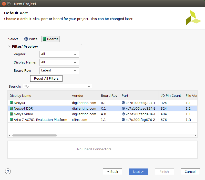
Ok, I want to tell you how we made these examples. First of all, we need a PC(Windows/Linux) that has min 30GB free space and a FPGA board. Our FPGA board mode is NEXYS 4 DDR. Step by step follow:
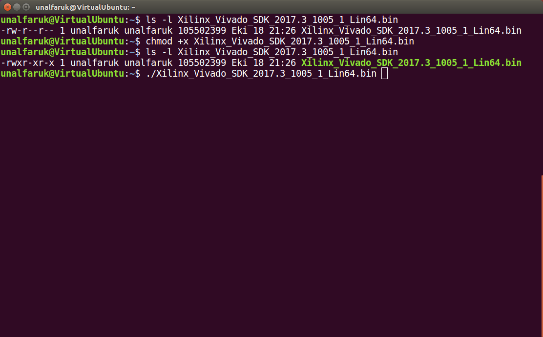
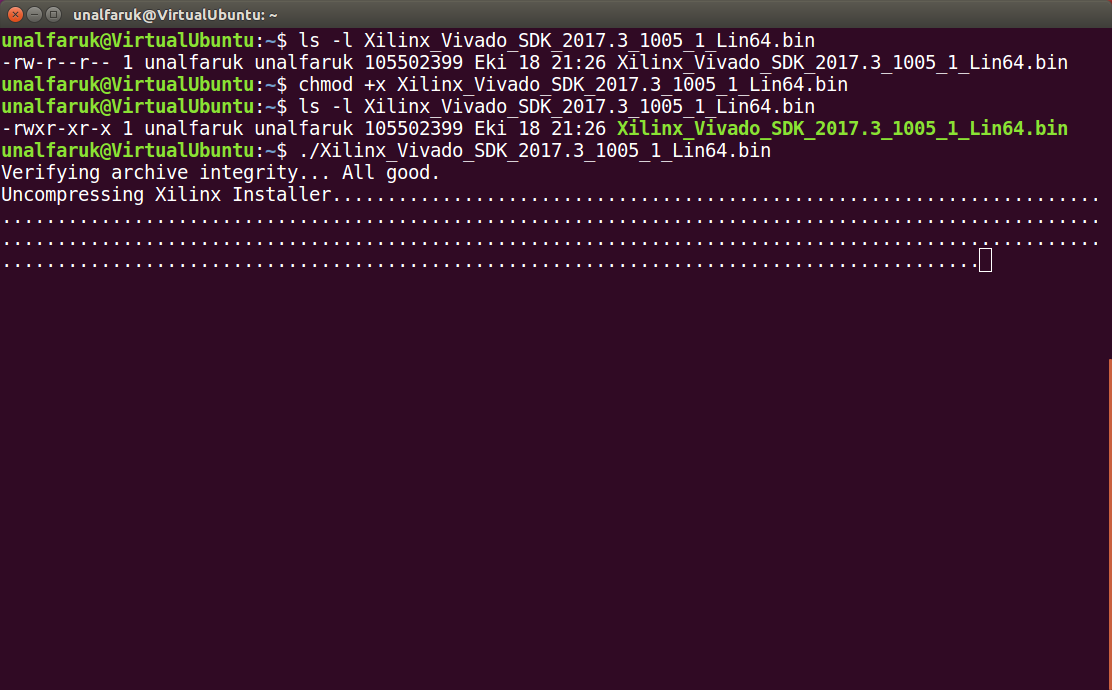
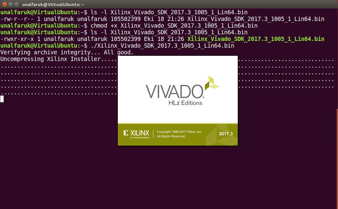
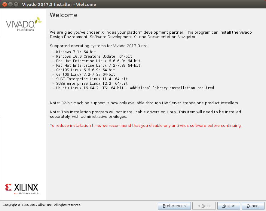
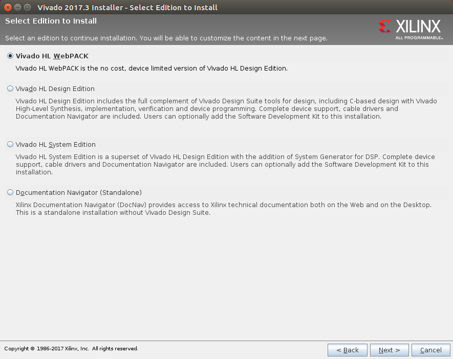
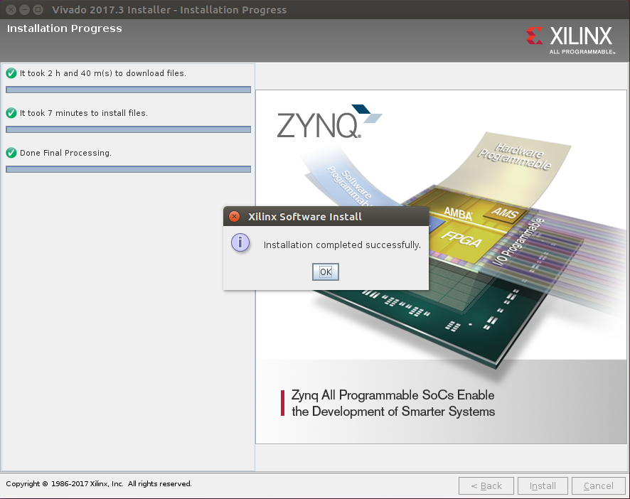
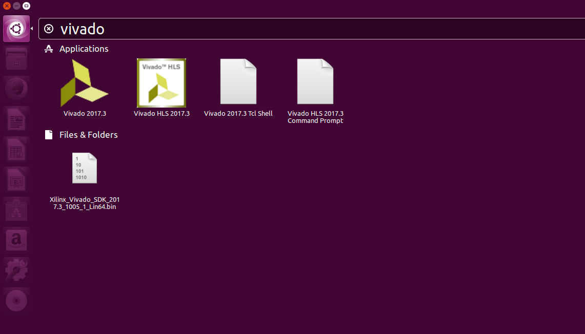
1 > Installation Vivado: Vivado is a customized text editor for FPGA. We can write a code, design a diagram etc. and generate codefile for FPGA. Computers that we used at lab were using Windows OS, but I want to tell for Linux OS (Ubuntu 16.04).
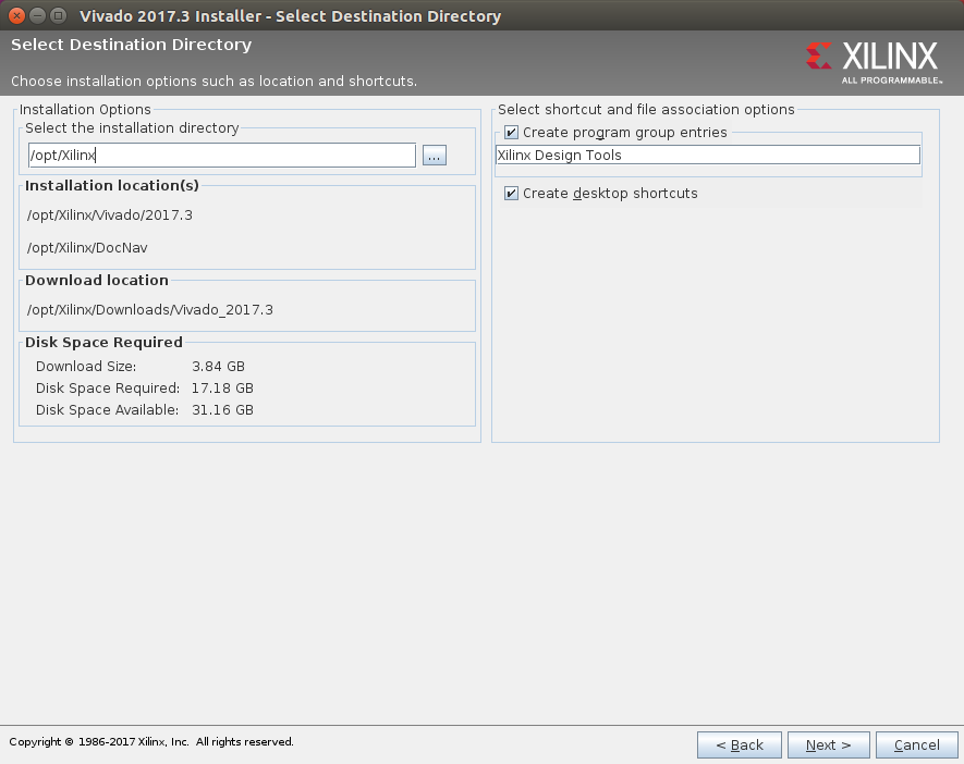
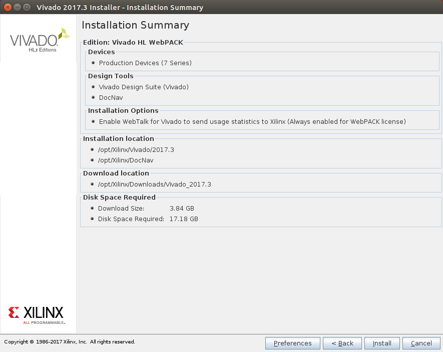
From this link, you can download “Vivado HLx 2017.3: WebPACK and Editions – Linux“. When download is complete, you have a file that it’s extension is “.bin”.
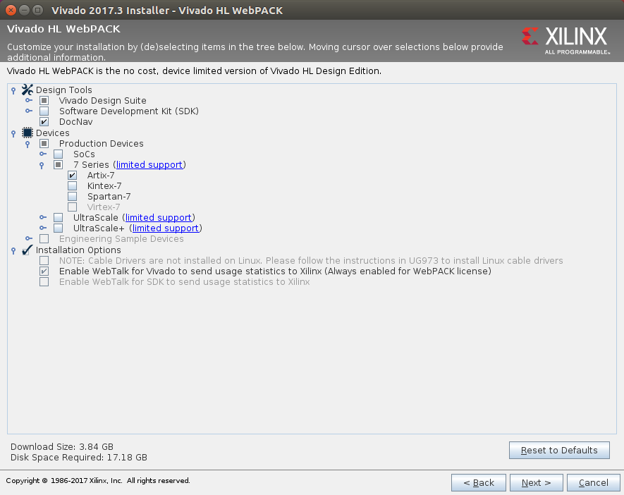
Warn: Before installation Vivado, learn FPGA model that using on your board. So you can save free space on disk.
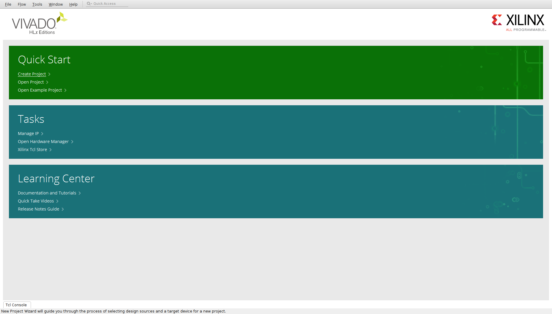
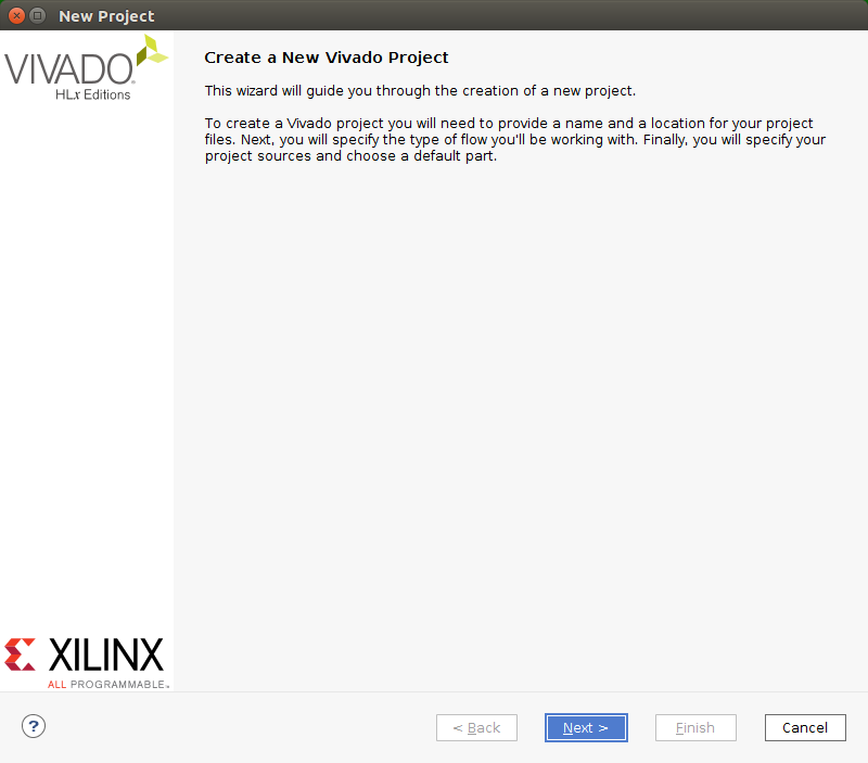
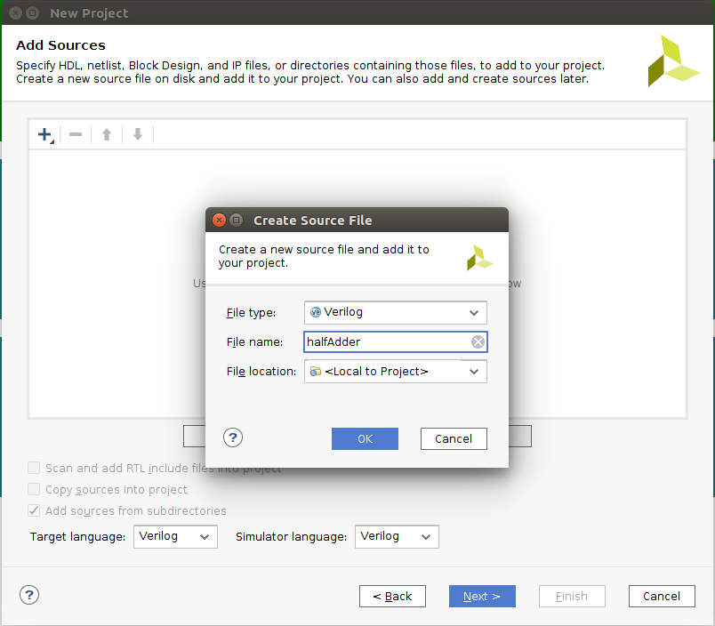
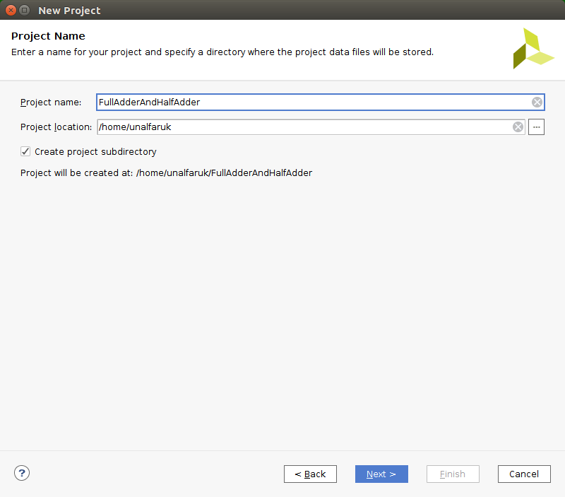
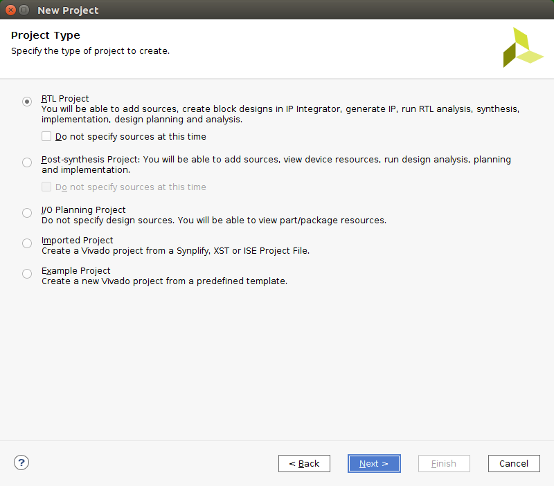
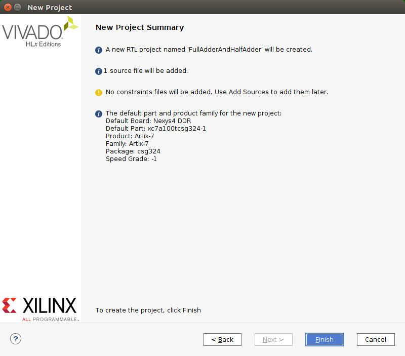
2 > Using Vivado (Half Adder Project): After installation, we can create projects and write codes and generate bitstream for load FPGA.
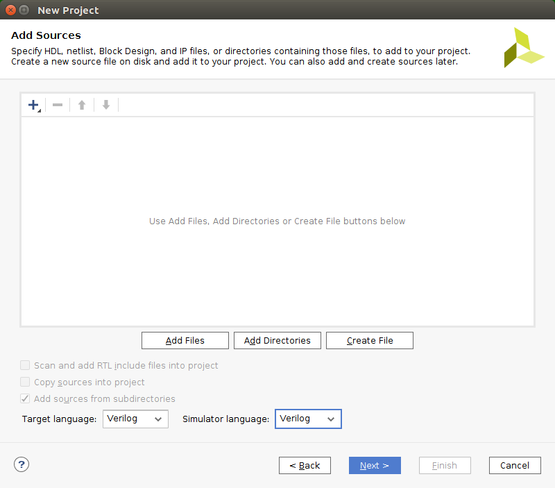
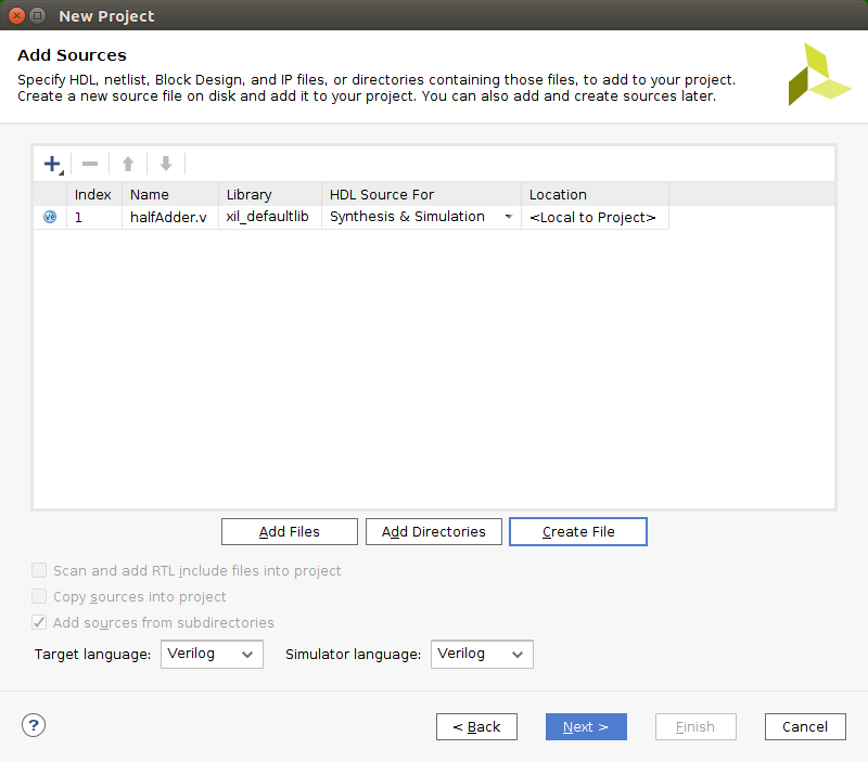
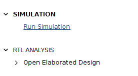
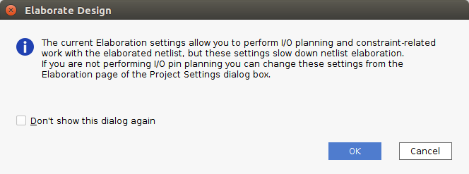
Warn: Pay attention to the sixth photo of the slide > Target language and simulation language.
We designed a full adder circuit, too. But I don’t want to tell that example in this post, I hope I’ll write this in next post.
Leave a Reply